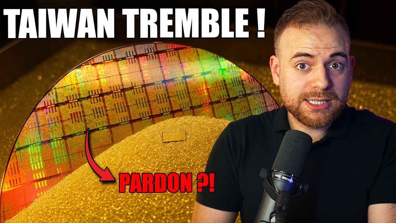
Voici le matériau chinois qui vient de tuer le silicium
Keywords
Summary
113 words
Critical Evaluation
The video provides a compelling and well-structured overview of the transition from silicon to 2D semiconductors, specifically MoS2. It effectively explains the physical limitations of silicon, the energy challenges in AI, and the recent breakthroughs in China and the US. The information is presented in an accessible manner, making complex topics understandable for a general audience. However, the video lacks detailed citations for many claims, relying on general references to ‘IMEC roadmap’ and ‘reports’ without specific sources. The narrative is somewhat one-sided, focusing on the potential of MoS2 without thoroughly discussing competing materials or the significant engineering hurdles that remain. The title is sensationalist, but the content is largely accurate. The video’s strength lies in its ability to contextualize technical developments within broader geopolitical and economic trends, offering a balanced view of the challenges and opportunities. The inclusion of specific examples, such as the Chinese pilot line and the US-based C Dimension, adds credibility. However, the lack of critical analysis of the feasibility of large-scale production and the potential for other materials to emerge is a notable omission. Overall, the video is informative and thought-provoking, but it would benefit from more rigorous sourcing and a more critical examination of the claims presented.
202 words
Title / Content Match
The title is somewhat sensationalist ('killed silicon') but the content accurately discusses the emergence of 2D materials as successors to silicon, aligning with the core message.
Quality & Reliability
7/10
The video provides a well-structured overview of the transition from silicon to 2D semiconductors, citing specific research and industrial developments. However, it lacks detailed citations for many claims and relies on a single narrative perspective, with some potential for oversimplification.
Chapters
Cited Sources
- Vision IA Newsletter — Mentioned as a free daily newsletter for AI news and ideas.
- Vision IA Training — Promoted as a comprehensive AI training program.
Concurring Sources
- IMEC Roadmap — The video references IMEC's roadmap predicting silicon's decline around 2041.
- Nature paper on MoS2 transistors — The video mentions Stanford and Chalmers publishing in Nature about MoS2 nanoribbon transistors.
Dissenting Sources
- Critique of 2D semiconductor scalability — Some experts argue that 2D materials face significant challenges in large-scale manufacturing, including uniformity and defect control, which may delay their adoption.
Contribution & Novelties
The video synthesizes recent developments in 2D semiconductors, particularly MoS2, and their potential to replace silicon. It highlights the geopolitical implications of bypassing EUV lithography and the race between China and the US. The video also introduces the concept of the ‘valley of death’ for new technologies, providing a framework for understanding the challenges ahead.
Pour aller plus loin :
- IMEC Roadmap — Official roadmap for semiconductor scaling.
- MoS2 transistor research — Recent Nature paper on MoS2 transistors.
- EUV lithography — ASML’s page on EUV technology.
86 words
Radar Profile
The radar profile shows a balanced distribution across all dimensions, with slightly higher scores in information quantity and technical level, indicating a well-rounded presentation. The lower score in reliability suggests room for improvement in sourcing and critical analysis.