반도체소자 Lecture1 2
Keywords
Summary
155 words
Critical Evaluation
Value of the Information & Strength of the Argument
The lecture provides valuable, practical knowledge about semiconductor manufacturing, with clear explanations of key concepts such as the Czochralski method and doping. The argumentation is solid, as the instructor builds on previous lessons and uses concrete examples, like calculating atomic density and segregation coefficients. However, the presentation is informal and lacks rigorous citations, which slightly weakens the scientific depth.
Scientific Rigor, Source Quality, Title Accuracy
The scientific rigor is moderate: the content is accurate but presented without formal references. The title accurately reflects the content, and the lecture is well-structured. No comments were provided, so public reception cannot be assessed.
109 words
Title / Content Match
The title accurately reflects the content, which is the second part of a semiconductor device lecture.
Quality & Reliability
7/10
The lecture provides a solid introduction to semiconductor materials and manufacturing processes, with accurate technical explanations and practical examples. However, it lacks citations and formal references, and the presentation is informal and conversational.
Key Moments
Markers derived by PSI from the transcript: the creator did not define chapters.
- Review of previous lecture on semiconductor basics and crystal structures.
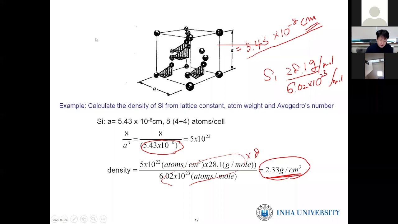
- Calculation of silicon atomic density using lattice constant.
- Discussion on the importance of high purity in semiconductors.
- Explanation of the Czochralski method for growing silicon ingots.
- Wafer slicing and polishing processes.
- Evolution of wafer sizes and economic benefits.
- Introduction to doping and segregation coefficients.
- Epitaxial growth methods: MBE and CVD.
- Application to solar cell manufacturing.
Contribution & Novelties
The lecture offers a comprehensive overview of silicon wafer manufacturing, from purification to wafer production, with practical insights into doping and epitaxy. It bridges theoretical concepts with industrial applications, making it useful for students and engineers.
Pour aller plus loin :
- Czochralski method — Detailed explanation of the crystal growth technique.
- Semiconductor device fabrication — Overview of the entire manufacturing process.
- Segregation coefficient — Concept used in doping control.
69 words
Radar Profile
The radar profile shows a balanced performance across all dimensions, with slightly higher scores in information quantity and reliability, reflecting the lecture's comprehensive yet informal nature.