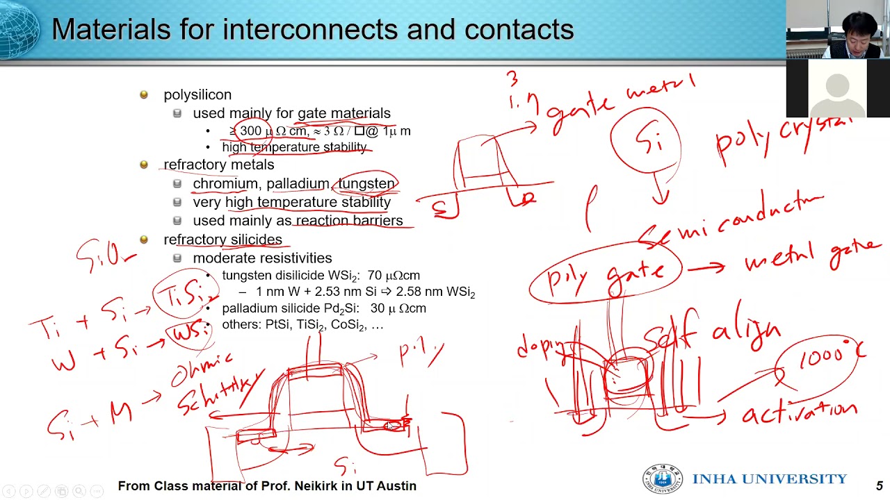
반도체공정 Lecture7 metallization 2 201118
Keywords
Summary
130 words
Critical Evaluation
Value of the Information & Strength of the Argument
The lecture provides valuable insights into the practical aspects of metallization in semiconductor manufacturing, explaining the rationale behind material choices and process steps. The argumentation is solid, grounded in physical principles and industry practices. The instructor effectively justifies the use of silicides, barrier layers, and specific deposition techniques, and addresses common failure mechanisms like spiking and electromigration. The content is well-structured, building from basic concepts to more complex integration issues.
Scientific Rigor, Source Quality, Title Accuracy
The lecture demonstrates scientific rigor in its technical explanations, but it does not cite specific external sources, relying instead on the instructor’s expertise. The title accurately reflects the content, which is a focused lecture on metallization. The absence of citations is typical for a lecture format, but it limits the ability to verify claims independently. The content aligns with established semiconductor manufacturing knowledge.
148 words
Title / Content Match
The title accurately reflects the content, which is a lecture on metallization processes in semiconductor fabrication.
Quality & Reliability
7/10
The lecture is a detailed technical exposition of metallization processes in semiconductor manufacturing, based on established engineering principles. The content is consistent with standard industry knowledge, but lacks explicit citations to external sources, relying on the instructor's expertise.
Key Moments
Markers derived by PSI from the transcript: the creator did not define chapters.
- Introduction to metallization and review of metals used in semiconductor interconnects.
- Discussion on the use of polysilicon for gates and the need for silicides to reduce contact resistance.
- Explanation of sputtering process and its advantages for depositing various metals.
- Comparison of sputtering and CVD, highlighting step coverage and film quality issues.
- Introduction to barrier and adhesion layers, and their importance in preventing diffusion.
- Discussion on contact and via formation, and the role of tungsten plugs.
- Explanation of aluminum spiking and the use of silicon doping to mitigate it.
- Detailed analysis of the aluminum-silicon phase diagram and solid solubility.
- Introduction to silicide formation and its benefits for contact resistance.
- Discussion on hillock formation and electromigration as reliability issues in aluminum interconnects.
Contribution & Novelties
The lecture provides a comprehensive overview of metallization processes, integrating material science and process engineering. It offers practical insights into the challenges of scaling and the solutions employed in industry. The discussion on silicide formation and the evolution from aluminum to copper interconnects is particularly informative.
Pour aller plus loin :
- Semiconductor device fabrication — Provides background on overall fabrication processes.
- Sputter deposition — Details the sputtering technique mentioned in the lecture.
- Electromigration — Explains the reliability phenomenon discussed in the lecture.
82 words
Radar Profile
The radar profile shows high scores in quantity of information and technical level, indicating a dense, technical lecture. Quality and reliability are slightly lower due to lack of citations, but still solid. The overall balance suggests a valuable educational resource for those with background in semiconductors.