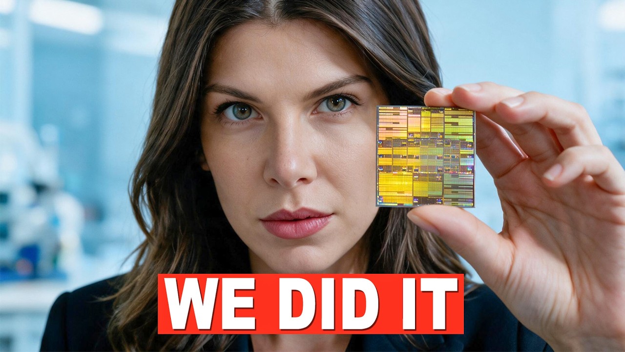
World's First 0.7 Nanometer Microchip
Keywords
Summary
156 words
Critical Evaluation
The video provides a clear and engaging explanation of a complex semiconductor manufacturing process. The presenter effectively breaks down the concept of wafer bonding and its significance, using analogies and visual aids. The technical details are generally accurate, though some simplifications are made for a general audience. The argumentation is solid, focusing on the manufacturing shift rather than just the headline transistor size, which adds depth. However, the video lacks direct citations to primary sources, relying instead on general industry knowledge and the presenter’s expertise. The promotional segment for Make, while clearly marked, interrupts the flow and may reduce perceived objectivity. The title accurately reflects the content, and the video does not overhype the technology, noting that mass production is still a challenge. Overall, the video is informative and well-presented, but viewers seeking rigorous scientific detail may need to consult additional sources.
142 words
Title / Content Match
The title accurately reflects the content, which focuses on IBM's 0.7nm microchip and its manufacturing innovation.
Quality & Reliability
7/10
The video presents a plausible explanation of IBM's 0.7nm chip announcement, focusing on wafer bonding and the Nanostack architecture. It includes technical details and references to industry labs (IMEC) and companies (EV Group, Tokyo Electron). However, it lacks direct citations to primary sources, and the promotional segment for Make reduces overall reliability.
Key Moments
Markers derived by PSI from the transcript: the creator did not define chapters.
- Introduction to IBM's 0.7nm chip announcement and the key innovation of wafer bonding.
- Explanation of the transistor structure with 15-atom-wide channels and the two-wafer approach.
- Discussion of the thermal challenges in building stacked transistors and the solution of separate wafer manufacturing.
- Explanation of Van der Waals forces and how they enable wafer bonding.
- Sponsored segment for Make, an AI automation tool.
- Discussion of contamination control and the importance of cleanrooms in wafer bonding.
- Examples of existing wafer bonding applications in camera sensors, HBM, and flash storage.
- Explanation of the Nanostack architecture and its potential benefits for AI performance and power efficiency.
- Conclusion on the future of chip manufacturing and the role of companies like EV Group and Tokyo Electron.
Cited Sources
- Anastasi In Tech Newsletter — Presenter's newsletter for further reading and updates.
- Deep in Tech Podcast on Apple — Podcast platform where the presenter discusses tech topics.
- Deep in Tech Podcast on Spotify — Podcast platform where the presenter discusses tech topics.
- Make (sponsor) — Sponsored link for Make, an AI automation tool mentioned in the video.
- Anastasi In Tech LinkedIn — Presenter's LinkedIn profile for professional networking.
Concurring Sources
- IBM Newsroom — Official IBM announcements may confirm the 0.7nm chip details.
- Semiconductor Engineering — Industry publication often covers wafer bonding and advanced packaging.
Dissenting Sources
- No specific discordant sources found — The video does not present controversial claims; however, some experts might argue that the 0.7nm label is marketing and not a physical dimension, which aligns with the video's own explanation.
Contribution & Novelties
The video provides a clear explanation of IBM’s 0.7nm chip announcement, focusing on the manufacturing innovation of wafer bonding rather than just the transistor size. It highlights the shift from shrinking transistors to stacking them, which is a significant conceptual change in semiconductor manufacturing. The presenter’s background as a chip design engineer adds credibility, and the video effectively communicates the technical challenges and potential benefits.
Pour aller plus loin :
- Wafer bonding — Provides a general overview of the technique used in the video.
- Van der Waals force — Explains the fundamental physics behind the bonding process.
- IBM Research — Official IBM research page where announcements and papers may be found.
- IMEC — Leading semiconductor research lab mentioned in the video.
- EV Group — Company specializing in wafer bonding equipment, mentioned as key for scaling.
135 words
Radar Profile
The radar profile shows high scores in quantity of information and technical level, indicating a detailed and technical presentation. Quality of information is good but slightly lower due to lack of direct citations. Overall reliability is moderate, reflecting the promotional segment and reliance on the presenter's expertise.
💬 Très positif : Sur les 30 commentaires analysés, le public exprime un enthousiasme marqué pour la clarté des explications et la passion de la présentatrice, avec plusieurs remarques sur la qualité de la vulgarisation et l'anticipation des futures avancées.