Low Temperature Plasma Processes: From Silicon Thin Films to Epitaxial Growth & Nanostructure for PV
Keywords
Summary
219 words
Critical Evaluation
Value of the Information & Strength of the Argument
The talk provides valuable insights into alternative photovoltaic technologies, particularly low-temperature plasma processes. The speaker’s argumentation is solid, based on his extensive research and published results. He systematically compares his approaches to conventional silicon technology, highlighting advantages in energy consumption, material usage, and scalability. He presents concrete data, such as efficiencies of 16.3% for triple-junction cells and 20% for heterojunction cells, and demonstrates the feasibility of low-temperature epitaxy and nanowire growth. The argumentation is persuasive, though it is primarily a personal perspective rather than a comprehensive review, and some claims could benefit from more detailed evidence.
105 words
Title / Content Match
The title accurately reflects the content, covering low-temperature plasma processes for silicon thin films, epitaxial growth, and nanostructures for photovoltaics.
Quality & Reliability
8/10
The speaker is a recognized expert in the field, with 30 years of experience, and presents results from his own research, including published data. The talk is a plenary at a scientific conference, indicating peer acceptance. However, it is a single perspective and not a systematic review, and some claims lack detailed citations.
Key Moments
Markers derived by PSI from the transcript: the creator did not define chapters.
- Introduction: speaker's background and overview of the talk.
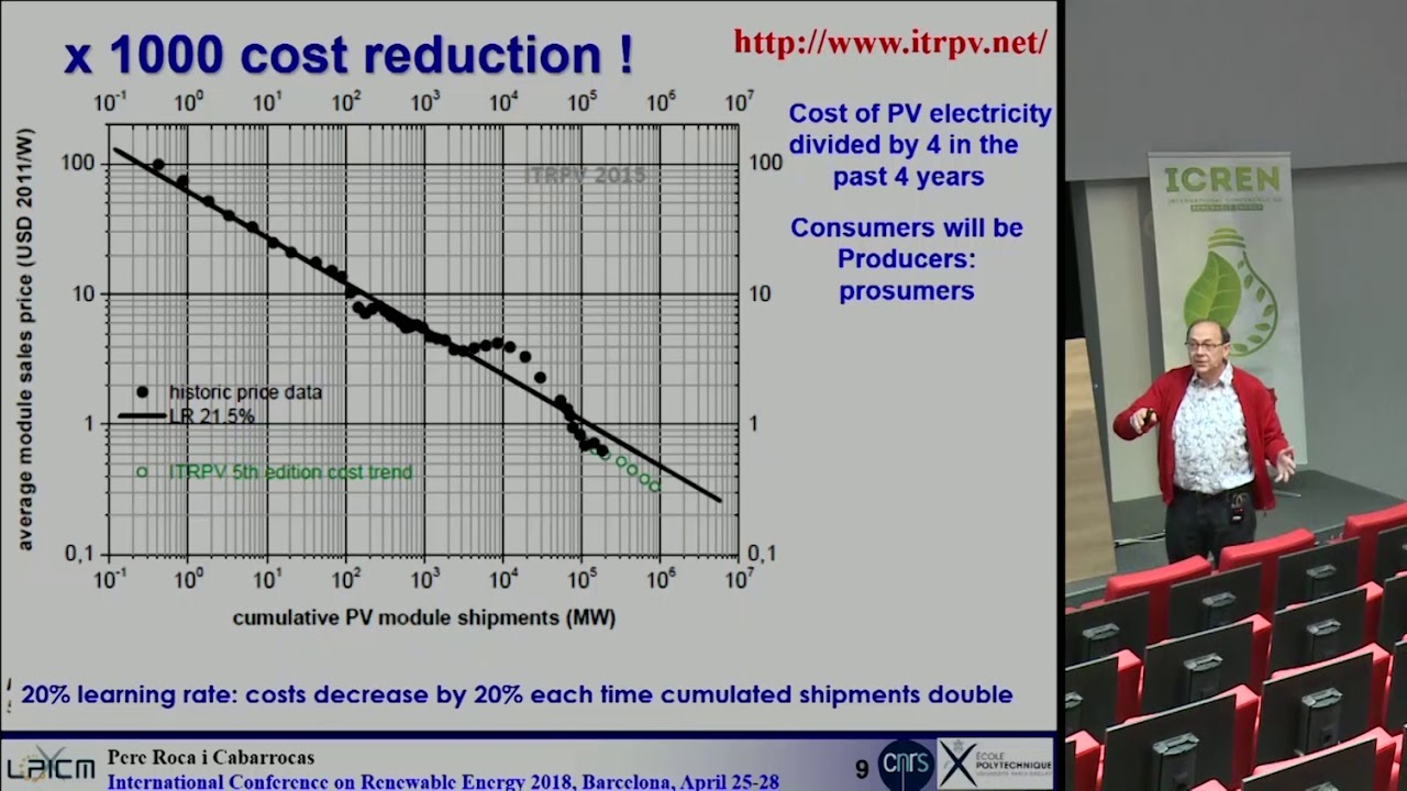
- Energy context: renewables share, PV potential, and cost reductions.
- Crystalline silicon dominance and its limitations for terawatt scale.
- Thin-film technologies: amorphous and microcrystalline silicon, tandem cells.
- Low-temperature epitaxy: growth of crystalline silicon on silicon, results.
- Epitaxial growth on foreign substrates: germanium on GaAs, potential for III-V on silicon.
- Silicon nanowire solar cells: growth, radial junctions, and tandem devices.
- Conclusion: future outlook and need for alternative technologies.
Cited Sources
- Renewable Energy International Conference 2018 — This is the video itself, where the talk was delivered.
Concurring Sources
- NREL Best Research-Cell Efficiency Chart — Provides efficiency records for various solar cell technologies, supporting the speaker's claims about record efficiencies.
Contribution & Novelties
The talk presents original research on low-temperature plasma processes for photovoltaic applications, including polymorphous silicon, low-temperature epitaxy, and silicon nanowire solar cells. The speaker demonstrates that high-quality crystalline silicon can be grown at 200°C using plasma-enhanced CVD, challenging conventional high-temperature processes. He also shows heteroepitaxy of germanium on GaAs, which could enable III-V on silicon tandem cells. The nanowire solar cells offer a novel approach to decouple light absorption and carrier collection, potentially reducing material usage. These contributions are significant for advancing thin-film PV technologies.
Pour aller plus loin :
- Plasma-enhanced chemical vapor deposition — Overview of PECVD technique.
- Heterojunction solar cell — Explanation of heterojunction concept.
- Silicon nanowire — Properties and applications of silicon nanowires.
116 words
Radar Profile
The radar profile shows high scores in quantity and quality of information, with a moderate technical level, indicating a talk that is informative and credible but not overly technical. The overall reliability is high, reflecting the speaker's expertise and the conference setting.