Moving Defect Detection And Classification To The Edge
Keywords
Summary
170 words
Critical Evaluation
Value of the Information & Strength of the Argument
The video provides valuable insights into the practical application of edge AI in semiconductor manufacturing, a topic of high industrial relevance. The argumentation is solid, based on real-world challenges and specific use cases, demonstrating the effectiveness of the approach. The expert’s explanations are clear and logical, supporting the claims with concrete examples. However, the content is promotional in nature, lacking independent validation or comparative analysis with alternative methods.
Scientific Rigor, Source Quality, Title Accuracy
The scientific rigor is moderate; the video presents expert opinion without formal citations or references to published studies. The sources cited are limited to the company’s own solutions and use cases, which may introduce bias. The title accurately reflects the content, and the discussion is technically sound but not exhaustive. No external sources are provided in the description, so the reliability relies on the expert’s credibility.
149 words
Title / Content Match
The title accurately reflects the content, which focuses on moving defect detection and classification to the edge.
Quality & Reliability
7/10
The video features an expert from Onto Innovation discussing practical applications of edge AI in semiconductor manufacturing. It provides specific use cases and technical details, but lacks formal citations or peer-reviewed references, and is a promotional interview.
Key Moments
Markers derived by PSI from the transcript: the creator did not define chapters.
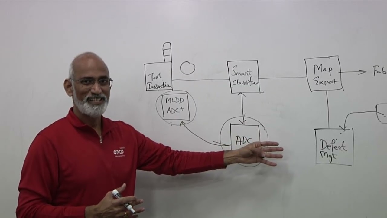
- Introduction and driver for moving defect detection to the edge.
- Explanation of image types and illumination modes.
- Discussion on defect explosion at 2nm and below.
- Challenge of nuisance defects and need for ML.
- Training ML models and IP protection.
- Use of GPUs and processing challenges.
- Inspection process flow and edge ADC.
- Human involvement in model deployment and updates.
- Use case 1: Low contrast defects in memory cells.
- Use case 2: Post-CMP whole wafer pattern detection.
- Use case 3: Grinding marks vs scratches on backside.
- Conclusion and summary.
Contribution & Novelties
The video provides a clear explanation of how edge AI is applied to semiconductor defect detection, addressing the data explosion challenge. It highlights the importance of distinguishing critical defects from nuisances and presents real-world use cases. The approach of moving AI to the edge is not entirely new but is well-articulated in this context.
Pour aller plus loin :
- Edge computing — Relevant for understanding the general concept of edge processing.
- Machine learning in semiconductor manufacturing — Provides background on the manufacturing process.
- Convolutional neural network — Key technique for image classification in defect detection.
95 words
Radar Profile
The radar profile shows balanced scores across information quantity, quality, technical level, and reliability, with a slight dip in reliability due to the promotional nature. This indicates a technically informative video with moderate scientific rigor.