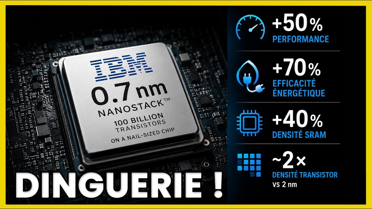
PANIQUE TOTALE chez AMD et INTEL : La techno secrète d'IBM arrive !
TOTAL PANIC at AMD and INTEL: IBM’s secret tech is here!
Title history
- PANIQUE TOTALE chez AMD et INTEL : La techno secrète d'IBM arrive ! — observed on 20261101-0112 UTC (YouTube)
Keywords
Summary
201 words
Critical Evaluation
Value of the Information & Strength of the Argument
The video offers informative value by demystifying the misconception around nanometer node names and explaining the novel concept of vertical transistor stacking. The argumentation is solid, as the presenter supports claims with logical reasoning and comparisons. For instance, he correctly points out that current node names do not correspond to physical gate lengths, using EUV lithography limitations (13.5nm wavelength) to illustrate this. He also provides a balanced view, acknowledging IBM’s progress while noting that TSMC remains the leader in production. However, the video lacks concrete citations to external sources, relying heavily on the presenter’s own analysis. The argumentation is coherent and accessible, avoiding unsubstantiated claims, though the tone occasionally leans toward sensationalism.
Scientific Rigor, Source Quality, Title Accuracy
The scientific rigor is moderate; the presenter accurately explains technical details but does not cite specific papers or official IBM documents. The quality of sources is limited to the announcement itself and general knowledge, with no named references in the video. The title is somewhat misleading, as it implies an immediate panic in the industry, whereas the content emphasizes that this is R&D and far from commercial reality. However, the video itself clarifies this, so the title overstates the urgency. The description links to a personal website without scientific references, offering little additional source material. Overall, the content is informative but not rigorously sourced.
231 words
Title / Content Match
The title is sensationalist ('TOTAL PANIC') but the content is more measured; it accurately describes IBM's technology and its potential impact on AMD and Intel, though the tone is exaggerated.
Quality & Reliability
7/10
The video provides accurate and up-to-date information on IBM's 0.7nm process announcement, with clear explanations of technical concepts. The presenter correctly clarifies the marketing nature of node names and distinguishes hype from actual innovation. However, the video relies mainly on the presenter's own interpretation without citing external sources beyond IBM's announcement, and some claims (e.g., exact performance gains) are presented without direct verification.
Key Moments
Markers derived by PSI from the transcript: the creator did not define chapters.
- Introduction to IBM's 0.7nm announcement and initial reaction
- Explanation that node names are technological generations, not physical dimensions
- Description of vertical transistor stacking concept using city analogy
- Discussion on SRAM cache and its importance for AI chips
- Comparison with TSMC's N2 node and differences in transistor architecture
- Challenges in production: cost, yield, foundry partnership
- Conclusion on future prospects and potential impact on consumer PCs
Cited Sources
- MakerTronic YouTube website — Mentioned in the video description as a resource for more detailed technical content.
Contribution & Novelties
The video’s original contribution is its accessible explanation of a complex semiconductor innovation, focusing on the conceptual shift from horizontal to vertical transistor stacking. It clarifies the marketing nature of node names, which is often misunderstood. The presenter also connects the technology to real-world applications, such as SRAM improvements for AI accelerators.
Pour aller plus loin :
- Gate-all-around transistors — Related concept explaining the current evolution of transistor architecture.
- Chip stacking — Overview of 3D integration, similar to IBM’s NanoStack approach.
- SRAM — Key memory component discussed, its role and challenges in modern processors.
94 words
Radar Profile
The radar chart would show a balanced profile with moderate-to-high scores across dimensions, reflecting a well-rounded but not exceptional video. The highest scores are likely in quantity of information and technical level, while rigor and novelty may be slightly lower due to lack of citations.