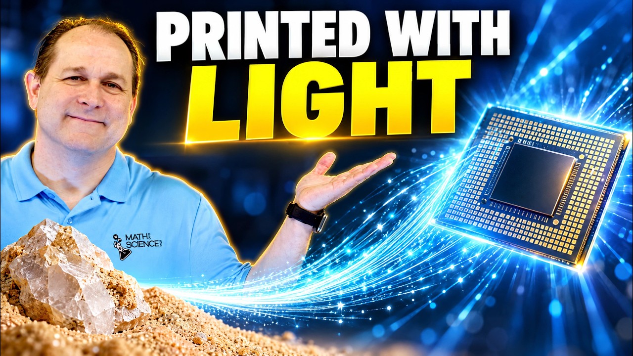
How Sand Becomes a Computer Chip
Keywords
Summary
200 words
Critical Evaluation
Value of the Information & Strength of the Argument
The video provides substantial value by demystifying a complex industrial process, breaking it down into comprehensible stages while maintaining scientific accuracy. The argumentation is clear and logical, progressing from raw materials through purification, crystallization, lithography, and final assembly. The use of analogies (e.g., ‘spray paint’ for photolithography, ‘paving stones’ for polysilicon) enhances understanding without oversimplifying. The explanation of why size reduction matters—more transistors, lower power, higher speed—is well articulated. The discussion of EUV, including the technical challenges and the near-monopoly of ASML, adds depth and current relevance. The argumentation is persuasive and backed by concrete examples (e.g., ENIAC vs. modern chips, Apple A17 Pro’s 19 billion transistors).
Scientific Rigor, Source Quality, Title Accuracy
The video demonstrates high scientific rigor by correctly describing processes like the Siemens process and Czochralski method, and by acknowledging the role of real companies and locations. It accurately differentiates between marketing labels (e.g., ‘3 nm’) and actual physical dimensions. The title is apt and effectively captures the video’s scope. The video does not cite specific academic sources, but it references industry-known facts and names of technology leaders (ASML, Zeiss, TSMC), which serves as implicit authoritative sourcing. The absence of cited literature is compensated by the specificity and technical correctness of the content. No critical inaccuracies or misleading claims were identified. The video also benefits from visual demonstrations and clear graphics that complement the verbal explanation.
238 words
Title / Content Match
The title accurately reflects the content, which traces the transformation of sand (quartz) into a finished computer chip. The video fully delivers on this promise.
Quality & Reliability
9/10
The video presents a well-structured, scientifically accurate explanation of semiconductor manufacturing. It references real companies (ASML, Zeiss, TSMC) and processes (Czochralski, photolithography, EUV) without notable factual errors. Some simplifications are inherent to the educational format, but the core information is reliable and up-to-date.
Key Moments
Markers derived by PSI from the transcript: the creator did not define chapters.
- Introduction to the myth of using beach sand and explanation of quartz as the true starting material.
- Description of the Siemens process to purify silicon and achieve electronic-grade purity.
- Czochralski crystal growth method producing a single large ingot.
- Overview of photolithography, including the role of masks and light in patterning wafers.
- Detailed explanation of EUV lithography, the need for vacuum and special mirrors, and ASML's dominant role.
- Final steps: testing, dicing, packaging, and the global supply chain that brings chips to consumers.
Cited Sources
- Extreme ultraviolet lithography — Mentioned in the video as the technology used for the smallest layers, with ASML as the sole producer.
- Czochralski method — Described as the process for growing single-crystal silicon ingots.
- ASML Holding — Identified as the Dutch company that builds EUV lithography machines.
- Zeiss — Mentioned as the German company producing ultra-smooth mirrors for EUV systems.
Contribution & Novelties
The video successfully condenses a highly technical field into an engaging and accurate narrative. It goes beyond the common statement that chips are made from sand by explaining the specific steps and the engineering challenges. It also clarifies misconceptions about transistor size and highlights the geopolitical and logistical aspects of semiconductor manufacturing, which are often omitted in similar educational content. The inclusion of ASML’s near-monopoly and the global supply chain adds a fresh perspective.
Pour aller plus loin :
- Moore’s Law — Discusses the observation that transistor density doubles approximately every two years, which drives the need for ever-smaller features.
- Semiconductor device fabrication — Provides a comprehensive overview of the entire manufacturing process, including details of photolithography and etching.
- Cleanroom — Explains the controlled environments essential to prevent contamination during chip production.
132 words
Radar Profile
The radar profile shows a balanced distribution across dimensions, with high scores in information quantity, quality, and reliability, and a slightly lower score in technical level. This indicates that the video is both comprehensive and trustworthy, while maintaining an accessible technical depth suitable for a broad audience.