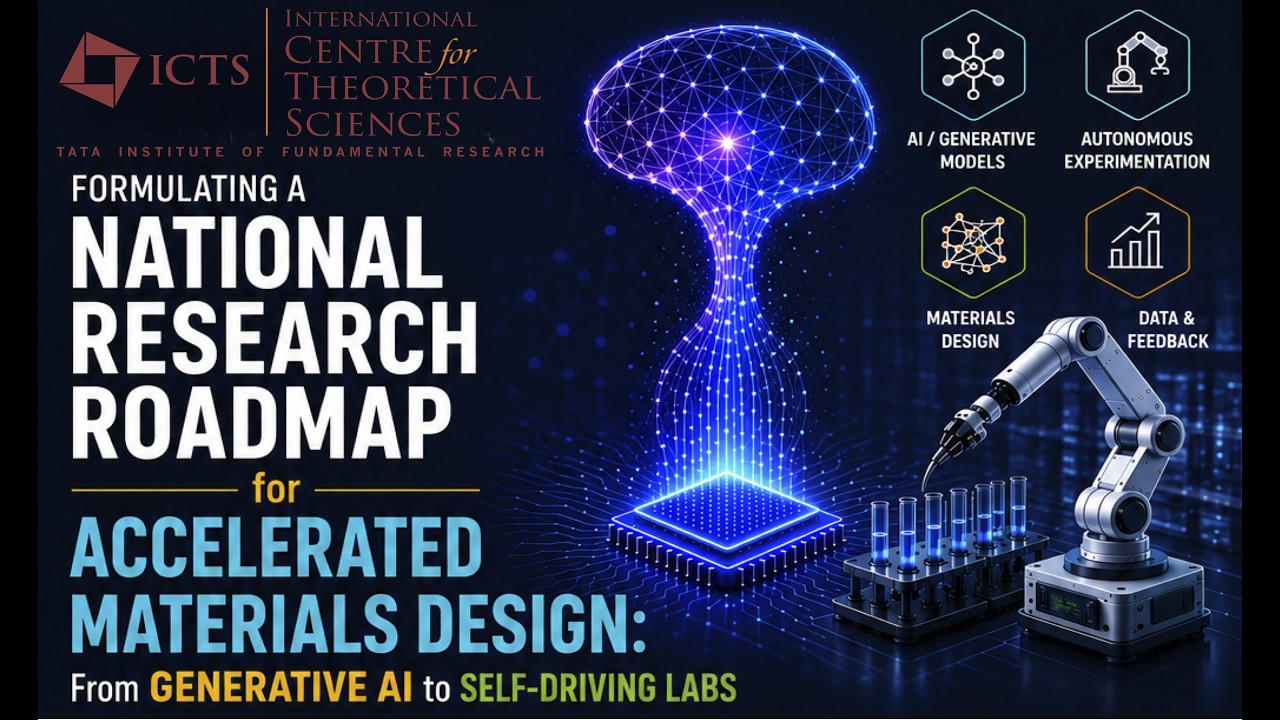
From Model to Manufacturing: Translating AI-accelerated Materials Design... by Suraj Rengarajan
Title history
- From Model to Manufacturing: Translating AI-accelerated Materials Design... by Suraj Rengarajan — observed on 20261030-1128 UTC (YouTube)
Keywords
Summary
203 words
Critical Evaluation
Value of the Information & Strength of the Argument
The talk provides valuable industry perspectives that are often missing in academic discussions. The speaker effectively argues that AI must consider the entire manufacturing context—process windows, stack interactions, and thermal budgets—not just idealized material properties. His reasoning is grounded in real-world constraints like copy-exact manufacturing and conservative adoption, making the argument compelling. However, the argumentation relies primarily on qualitative experience, lacking concrete case studies or quantified outcomes, which limits its persuasive power for a technical audience.
Scientific Rigor, Source Quality, Title Accuracy
The presentation is rigorous in its use of industry-specific terminology and practical insights, but scientific citations are sparse; only the program link is provided in the description. The speaker mentions a recent publication from JNCSR on a high ZT material without formal reference, weakening the scientific grounding. The title aligns well with the content, capturing both the model-to-manufacturing theme and the role of AI. No comments were provided for analysis.
161 words
Title / Content Match
The title accurately reflects the presentation's focus on taking AI-driven materials design into semiconductor manufacturing.
Quality & Reliability
7/10
The talk offers practical industrial insights from a senior technologist, but relies on anecdotal evidence and lacks detailed quantitative data or peer-reviewed citations.
Key Moments
Markers derived by PSI from the transcript: the creator did not define chapters.
- Introduction of speaker and Applied Materials
- Industry perspective: not seeking best material, but consistent performance at scale
- Materials as part of a stack; 3,000 process steps
- Challenges in measuring non-bulk properties and process-dependent behavior
- AI applications in interconnect, ALD, and thermal interface materials
- Material screening funnel and role of AI in narrowing candidates
- Industry-academia collaboration: validation and scaling gaps in India
- Call for shared facilities, pilot lines, and increased interchange
Cited Sources
- Discussion Meeting: Formulating a National Research Roadmap for Accelerated Materials Design — Official program page for the discussion meeting where this talk was presented.
Contribution & Novelties
The talk contributes an industrial insider’s view of the barriers to adopting AI-designed materials, particularly the need for process integration and scale-up. It underscores that materials must be valid across entire process flows, not just in isolation. The proposal for shared pilot lines and stronger academia-industry partnerships offers a pragmatic path forward for India’s semiconductor ambitions.
Pour aller plus loin :
- Atomic layer deposition — Relevant to the speaker’s discussion of ALD challenges and precursors.
- Semiconductor device fabrication — Provides background on the many process steps that materials must survive.
- Materials informatics — Directly relates to the use of AI and data-driven methods in materials design.
106 words
Radar Profile
The profile shows a moderate balance across all dimensions, with slightly higher scores in quality and reliability. The technical level and information quantity are adequate but not exceptional, reflecting a high-level overview rather than a deep dive.